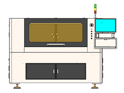
Coating bonding strength nondestructive testing instrument is a nondestructive testing equipment that uses the interaction mechanism between coating material and workpiece substrate by high-frequency ultrasonic pulse echo to determine the bonding strength. The function of graded determination of coating bonding strength can be implemented for workpieces with a difference of acoustic impedance between coating and substrate of more than 10 times. It is suitable for testing the bonding strength of polymer or composite coatings of various metal based workpieces.
The detection instrument also has the function of ultrasonic microscope. Through ultrasonic imaging of fine structures or defects in the workpiece, it can detect defects such as cracks, delaminations and cavities in the material. Semiconductor and microelectronics are widely used in quality inspection of chip brazing defects, electronic packaging defects, flexible circuit board disconnection and so on; The welding field can be used for quality inspection of spot welding, arc welding, laser welding, diffusion welding and so on. It supports xyzab axis five axis linkage, and can detect disk workpieces and workpieces with complex surfaces.
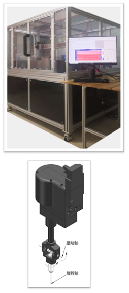
Main Specifications:
Mechanical motion part:
■ multi axis motion control system, linear motor is selected for XY axis, grating closed-loop control, grating ruler resolution 1 μ m
■ X-axis stroke: 400mm;
■ Y-axis stroke: 400mm;
■ z-axis stroke: 50mm;
■ probe angle adjustment: manual or electric AB axis;
Ultrasonic instrument sensor:
■ pulse excitation voltage: 100-475v; 200-900v optional;
■ system passband: 0.1-35mhz; 1-60MHz; 5-300MHz
■ sampling frequency: adjustable from 100MHz to 1GHz;
■ repetition frequency: high energy 5KHz; Low energy 20 kHz;
■ sampling depth: 8 or 14 bits;
■ high frequency focusing transducer: 100MHz or 150MHz
Some functions of software:
■ grating position precise trigger, minimum 10 μ M sampling interval;
■ DMA high-speed data transmission, full wave data acquisition, gate dynamic reconstruction;
■ multiple display modes of ABCD signal and image;
■ time domain signal peak, phase imaging, frequency domain peak and other imaging modes;
■ multi gate setting, surface wave or bottom wave gate following;
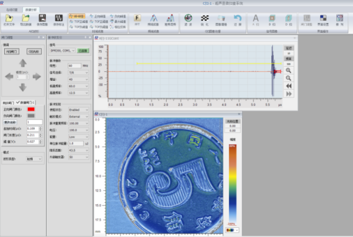
Software interface
Coating adhesion test:
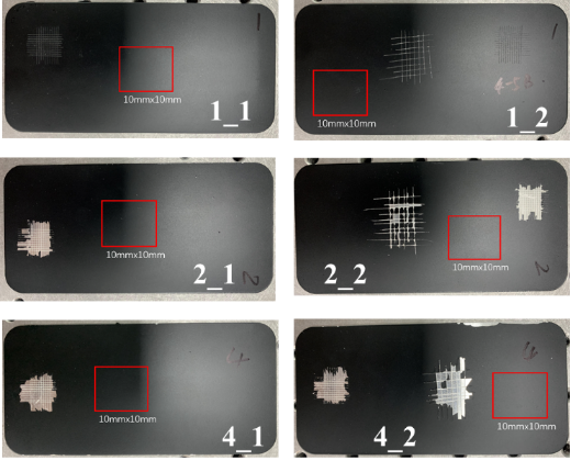
Photo of actual sample for aluminum base test
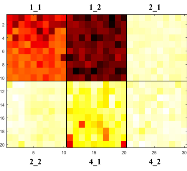
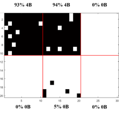
Maximum imaging of aluminum based test samples and
discrimination of bonding strength of aluminum based test samples
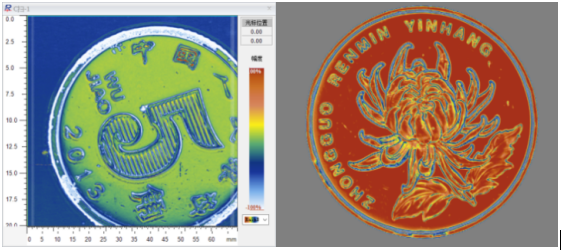
Coin ultrasonic imaging:
Chip detection:

Physical optical photos ultrasonic C-scan
Chip layered imaging:
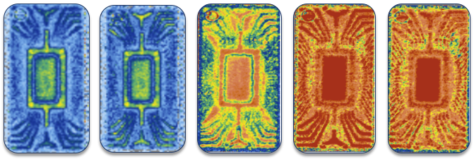
Layered C-scan image
Flexible circuit detection:

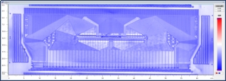
Physical optical photos ultrasonic C-scan

 +86 4000-198-196


 Hotline